Well, I figured what is the point of having all these lasers without snapping a few cool pics. :)
The green laser is a DPSS 10W puppy, the red is a 1mW He-Ne and the Blue light is a result of second harmonic generation by a periodically poled Lithium Niobate crystal.
Go to ImageShack® to Create your own Slideshow
Saturday, October 27, 2007
Antec 900 Case
A few pictures of MY Antec 900. It feels a bit cramped, but with all those humongous fans, it runs bloody cool!
Go to ImageShack® to Create your own Slideshow
Go to ImageShack® to Create your own Slideshow
Integrated Memory controller and its impact on Overclocking
I've noticed that Intel is more tolerant when it comes to populating all 4 DIMM slots. I was pleasantly surprised to find out that going from 2 x 1Gb to 4 x 1Gb necessitated no change in timings, voltages or anything else. Intel Tech docs said that modules can be run as a mix-n-match of single and dual channel SIMULTANEOUSLY. Now this is something very interesting and lacking with AMD. Is this the norm with Intel or am I just plain lucky?
So my question would be, is the AMD IMC really all that great as it is made out to be from an enthusiast perspective?
Check these out! Not bad for 2 x $60 sets huh?
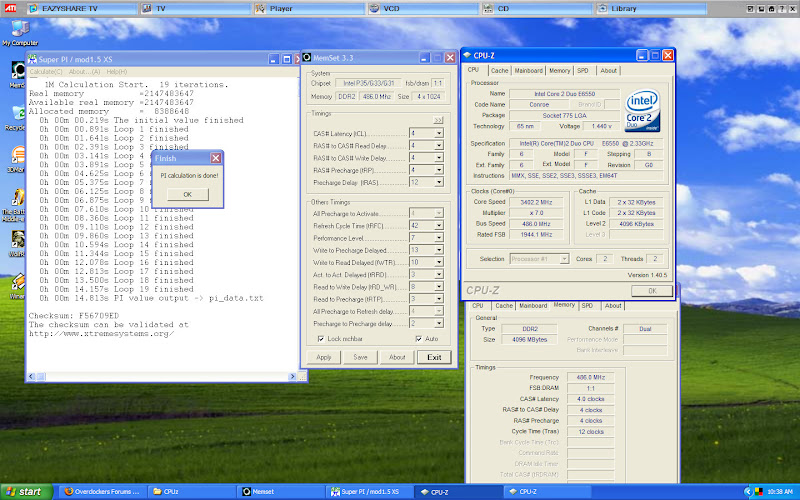
A friend of mine with an AM2 system could not even get his rig to POST at the same timings. Although an IMC would probably do a lot towards increased memory throughput (a rather loose term in itself), I believe it would also hamper system stability in overclocked machines.
I still need more data and ideas on how to actually support my speculation...
So my question would be, is the AMD IMC really all that great as it is made out to be from an enthusiast perspective?
Check these out! Not bad for 2 x $60 sets huh?
A friend of mine with an AM2 system could not even get his rig to POST at the same timings. Although an IMC would probably do a lot towards increased memory throughput (a rather loose term in itself), I believe it would also hamper system stability in overclocked machines.
I still need more data and ideas on how to actually support my speculation...
Buck Regulators
This article was originally published on overclockers.com. I'm no Power-Electronics Whiz and there may be a few mistakes in here. This is merely a short compendium of material for my reference!
Introduction:
Buck regulators are what provide DC power the CPU and DRAM and are the target of every Volt-modder. Volt modding in essence involves making available a voltage range beyond what is specified in the BIOS. While the BIOS allows a measure of voltage controlled vied the programmable nature of the buck regulator, going beyond the specs of the regulator itself is not possible in this manner. One could say we are overvolting the regulator or modifying the power supply loop characteristics to accommodate our needs. To attempt such a thing, we have to understand the basics of the component we are trying to mod. Linear voltage supplies/regulators have been around for quite a while. However, they bring with them several critical drawbacks such as low efficiency, which in turn necessitates the use of bulky heatsinks, cooling fans and isolation transformers. This in turn makes them unsuitable in today's world of compact electronic systems. The disadvantages of a linear power supply are greatly reduced by the use of an alternative scheme i.e regulated switching power supply. This brief note will discuss one such power supply, i.e the Buck-Regulator.
Buck regulators are what provide DC power the CPU and DRAM and are the target of every Volt-modder. Volt modding in essence involves making available a voltage range beyond what is specified in the BIOS. While the BIOS allows a measure of voltage controlled vied the programmable nature of the buck regulator, going beyond the specs of the regulator itself is not possible in this manner. One could say we are overvolting the regulator or modifying the power supply loop characteristics to accommodate our needs. To attempt such a thing, we have to understand the basics of the component we are trying to mod. Linear voltage supplies/regulators have been around for quite a while. However, they bring with them several critical drawbacks such as low efficiency, which in turn necessitates the use of bulky heatsinks, cooling fans and isolation transformers. This in turn makes them unsuitable in today's world of compact electronic systems. The disadvantages of a linear power supply are greatly reduced by the use of an alternative scheme i.e regulated switching power supply. This brief note will discuss one such power supply, i.e the Buck-Regulator.
What is wrong with a linear regulator?
Linear regulators are o.k for powering very low powered devices and devices which are not sensitive to thermal fluctuations. They are easy to use and cheap, and therefore are very popular. However, due to the way they work, they are extremely inefficient. A linear regulator works by taking the difference between the input and output voltages, and just burning it up as waste heat. The larger the difference between the input and output voltage, the more heat is produced. In most cases, a linear regulator wastes more power stepping down the voltage than it actually ends up delivering to the target device! With typical efficiencies of 40%, and reaching as low as 14%, linear voltage regulation generates a lot of waste heat which must be dissipated with bulky and expensive heatsinks.Even the new LDO (low drop-out) regulators are still inefficient linear regulators; They just give you more flexibility with input voltage drops.
Linear regulators are o.k for powering very low powered devices and devices which are not sensitive to thermal fluctuations. They are easy to use and cheap, and therefore are very popular. However, due to the way they work, they are extremely inefficient. A linear regulator works by taking the difference between the input and output voltages, and just burning it up as waste heat. The larger the difference between the input and output voltage, the more heat is produced. In most cases, a linear regulator wastes more power stepping down the voltage than it actually ends up delivering to the target device! With typical efficiencies of 40%, and reaching as low as 14%, linear voltage regulation generates a lot of waste heat which must be dissipated with bulky and expensive heatsinks.Even the new LDO (low drop-out) regulators are still inefficient linear regulators; They just give you more flexibility with input voltage drops.
How is a switching regulator better?
A switching regulator works by taking small chunks of energy, bit by bit, from the input voltage source, and moving them to the output. This is accomplished with the help of an electrical switch and a controller which regulates the rate at which energy is transferred to the output (hence the term “switching regulator”).The energy losses involved in moving chunks of energy around in this way are relatively small, and the result is that a switching regulator can typically have 85% efficiency. Since their efficiency is less dependent on input voltage, they can power useful loads from higher voltage sources. Switch-mode regulators are used in devices like portable phones, video game platforms, robots, digital cameras, and your computer. Switching regulators are complex circuits to design, and as a result they are not very popular with hobbyists.
What can switching regulators do that linear regulators can't?
With high input voltages, driving loads over 200 mA with a linear regulator becomes extremely impractical. A switching regulator can easily power heavy loads from a high voltage.Certain kinds of switching regulators can also step up voltage. Linear regulators cannot do this. Ever. So, switching regulators are used to provide clean DC output to the CPU and DRAM.
How do I tell if I need a switching regulator?
As a general rule of thumb, if your linear voltage regulation solution is wasting less than 0.5 watts of power, a switching regulator would be overkill for your project. If your linear regulator is wasting several watts of power, you most certainly want to replace it with a switcher!
Here is how to calculate power losses:
The equation for wasted power in a linear regulator is:
Power wasted = (Input voltage – output voltage) * load current
For example, let’s say you have a 12V lead-acid battery and you want to power a microcontroller that draws 5 mA, and an ultrasonic rangefinder that draws 50 mA. Both the microcontroller and the ultrasonic rangefinder run off of 5V. You use an LM7805 (a very common linear regulator) to get the voltage down to 5V from 12V.
Power wasted = (12V – 5V) * (0.050A + 0.005A) = 0.385W
0.385W is not too bad for power losses. The LM7805 can handle this without a big heatsink. You could get more battery life if you used a switching regulator, but in this case the power consumption is so low that the battery life will be very long anyway.
Now let’s expand on this example, and add two servos that draw an average of 0.375A each, and also run off of the 5V supply. How much power is wasted in a linear regulator now?
Power wasted = (12V – 5V) * (0.050A + 0.005A + 0.375A + 0.375A) = 5.635W
5.6 Watts is a lot of waste heat! Without a large heatsink the LM7805 would get so hot it would desolder itself or melt your breadboard. Even with the heatsink, 5.6W is also a lot of life to suck out of your battery for no reason. A switching regulator such as a DE-SW050 would be very useful in this case, and would reduce power losses to around 0.5W.
Pulse Width Modulation Basics:All of the switching converters described here use a form of output voltage regulation known as Pulse Width Modulation (PWM). Put simply, the feedback loop adjusts (corrects) the output voltage by changing the ON time of the switching element in the converter.As an example of how PWM works, we will examine the result of applying a series of square wave pulses to an L-C filter.
Buck Regulators: They are used to reduce a DC Voltage to a lower reference DC Voltage.The most commonly used switching converter is the Buck, which is used to down-convert a DC voltage to a lower DC voltage of the same polarity.This is essential in systems that use distributed power rails (like 24V to 48V),which must be locally converted to 15V, 12V or 5V with very little power loss.The Buck converter uses a transistor as a switch that alternately connects and disconnects the input voltage to an inductor.
 The series of square wave pulses is filtered and provides a DC output voltage that is equal to the peak pulse amplitude multiplied times the duty cycle (duty cycle is defined as the switch ON time divided by the total period).This relationship explains how the output voltage can be directly controlled by changing the ON time of the switch.
When the switch turns on, the input voltage is connected to the inductor. The difference between the input and output voltages is then forced across the inductor,causing current through the inductor to increase.During the on time, the inductor current flows into both the load and the output capacitor (the capacitor charges during this time).When the switch is turned off, the input voltage applied to the inductor is removed. However, since the current in an inductor can not change instantly, the voltage across the inductor will adjust to hold the current constant. The input end of the inductor is forced negative in voltage by the decreasing current, eventually reaching the point where the diode is turned on. The inductor current then flows through the load and back through the diode. The capacitor discharges into the load during the off time, contributing to the total current being supplied to the load (the total load current during the switch off time is the sum of the inductor and capacitor current).

As explained, the current through the inductor ramps up when the switch is on, and ramps down when the switch is off. The DC load current from the regulated output is the average value of the inductor current. The peak-to-peak difference in the inductor current waveform is referred to as the inductor ripple current, and the inductor is typically selected large enough to keep this ripple current less than 20% to 30% of the rated DC current.In most Buck regulator applications, the inductor current never drops to zero during full-load operation (this is defined as continuous mode operation). Overall performance is usually better using continuous mode, and it allows maximum output power to be obtained from a given input voltage and switch current rating. In applications where the maximum load current is fairly low, it can be advantageous to design for discontinuous mode operation. In these cases, operating in discontinuous mode can result in a smaller overall converter size (because a smaller inductor can be used). Discontinuous mode operation at lower load current values is generally harmless, and even converters designed for continuous mode operation at full load will become discontinuous as the load current is decreased (usually causing no problems).
The I/O characteristics of all DC-DC converters can be examined by using the requirement that the initial and final Inductor current within a period/cycle should be constant (i.e net energy stored in an inductor is zero). So, average voltage per cycle is zero. Mathematically:
Practical Constant ON-Time Buck Regulator (an example) :

The basic regulator IC consists of a comparator with input hysteresis that compares the output feedback voltage with a reference volt turning off the buck switch MOSFET.When the feedback voltage exceeds the reference voltage, the comparator output goes low, turning off the buck switch MOSFET. The switch remains off until the feedback voltage falls below the reference hysteresis voltage. Then, the comparator output goes high, turning on the switch and allowing the output voltage to rise again. It reacts extremely quickly to load and line transients due to its wide bandwidth control loop. Unlike a pulse width modulation (PWM) regulator, this loop does not require an error amplifier or frequency compensation.
Two PWM Control Techniques in Brief:
This is the most important part of a Buck regulator from an overclocker's standpoint. We had already hinted at this when calculating the output voltage and its dependence on the Duty cycle. In brief, by varying the ON time, the conduction of the transistor is increased and correspondingly the output voltage increases. The control circuitry senses any change in output voltage and adjusts the duty cycle to correct such changes. An oscillator sets the chopping frequency of the converter and a stable temperature compensated reference is used, to which, the output voltage is compared by a high gain error amplifier. An error voltage to the PWM is used to adjust the duty cycle. Feedback compensation techniques are nothing new and this is also known as a servo system. Usually a "servo" system has an error amplifier, integrator and a low pass filter in a feedback configuration.The two most common forms of control in dc/dc switching power converters are CM (current-mode) and VM (voltage-mode) control. Each method has its own advantages and disadvantages. CM control provides the ease of loop compensation and inherent line feed-forward, which makes this method a favorite among designers. VM control is more immune to noise. This characteristic is important in large-step-down-ratio applications in which the switch has a short on-time that is susceptible to noise pickup. The ideal approach that has been eluding designers is a practical CM-controlled regulator without noise-susceptibility challenges.
Voltage mode:
This is the more traditional mode of control in PWM switching converters. In a simple circuit, the components are an oscillator, an error amplifier and a comparator. The output voltage is sensed with respect to a reference and the error voltage is amplified by a high gain amplifier, this is followed by a comparator which compares the amplified error signal with a sawtooth waveform generated across a timing capacitor.
Let us take a look at the following schematic:

The circuit shown below is a voltage-mode PWM controller in which the error amplifier output is compared to a voltage ramp from the oscillator to determine the output pulse width. A current mode PWM replaces the oscillator ramp with a ramp that is proportional to the current in the magnetic element. A nice place to perform a mod would be to add a DC Bias voltage to the Voltage reference. It would be the easiest to do. Tweaking the compensation network would be a bit more involved as it can lead to huge output instability, resonance and ringing. It is not recommended that one messes with the feedback loop without any calculations.
Current Mode:
This is a more complicated multi-loop control technique, which has an AC current feedback loop (AC=oscillating current) in addition to the voltage feedback loop. The second loop controls the peak inductor current with the error signal rather than controlling the duty cycle of the switching waveform. This is an attractive option in high frequency switching applications.
To be continued....
References:
[1] http://www.dimensionengineering.com/switchingregulators.htm)
[2] http://www.elecdesign.com/Articles/ArticleID/12253/12253.html)
[3] PWM, Linear Technology App Notes)
[4] Power Electronics Design Handbook- Nihal Kulratna.
[5] Maxim-Dallas Semiconductor Application Notes
When the switch turns on, the input voltage is connected to the inductor. The difference between the input and output voltages is then forced across the inductor,causing current through the inductor to increase.During the on time, the inductor current flows into both the load and the output capacitor (the capacitor charges during this time).When the switch is turned off, the input voltage applied to the inductor is removed. However, since the current in an inductor can not change instantly, the voltage across the inductor will adjust to hold the current constant. The input end of the inductor is forced negative in voltage by the decreasing current, eventually reaching the point where the diode is turned on. The inductor current then flows through the load and back through the diode. The capacitor discharges into the load during the off time, contributing to the total current being supplied to the load (the total load current during the switch off time is the sum of the inductor and capacitor current).
As explained, the current through the inductor ramps up when the switch is on, and ramps down when the switch is off. The DC load current from the regulated output is the average value of the inductor current. The peak-to-peak difference in the inductor current waveform is referred to as the inductor ripple current, and the inductor is typically selected large enough to keep this ripple current less than 20% to 30% of the rated DC current.In most Buck regulator applications, the inductor current never drops to zero during full-load operation (this is defined as continuous mode operation). Overall performance is usually better using continuous mode, and it allows maximum output power to be obtained from a given input voltage and switch current rating. In applications where the maximum load current is fairly low, it can be advantageous to design for discontinuous mode operation. In these cases, operating in discontinuous mode can result in a smaller overall converter size (because a smaller inductor can be used). Discontinuous mode operation at lower load current values is generally harmless, and even converters designed for continuous mode operation at full load will become discontinuous as the load current is decreased (usually causing no problems).
The I/O characteristics of all DC-DC converters can be examined by using the requirement that the initial and final Inductor current within a period/cycle should be constant (i.e net energy stored in an inductor is zero). So, average voltage per cycle is zero. Mathematically:
VLOND + VLOff (1-D) = 0, where D is the duty cycle.
Practical Constant ON-Time Buck Regulator (an example) :
The basic regulator IC consists of a comparator with input hysteresis that compares the output feedback voltage with a reference volt turning off the buck switch MOSFET.When the feedback voltage exceeds the reference voltage, the comparator output goes low, turning off the buck switch MOSFET. The switch remains off until the feedback voltage falls below the reference hysteresis voltage. Then, the comparator output goes high, turning on the switch and allowing the output voltage to rise again. It reacts extremely quickly to load and line transients due to its wide bandwidth control loop. Unlike a pulse width modulation (PWM) regulator, this loop does not require an error amplifier or frequency compensation.
Two PWM Control Techniques in Brief:
This is the most important part of a Buck regulator from an overclocker's standpoint. We had already hinted at this when calculating the output voltage and its dependence on the Duty cycle. In brief, by varying the ON time, the conduction of the transistor is increased and correspondingly the output voltage increases. The control circuitry senses any change in output voltage and adjusts the duty cycle to correct such changes. An oscillator sets the chopping frequency of the converter and a stable temperature compensated reference is used, to which, the output voltage is compared by a high gain error amplifier. An error voltage to the PWM is used to adjust the duty cycle. Feedback compensation techniques are nothing new and this is also known as a servo system. Usually a "servo" system has an error amplifier, integrator and a low pass filter in a feedback configuration.The two most common forms of control in dc/dc switching power converters are CM (current-mode) and VM (voltage-mode) control. Each method has its own advantages and disadvantages. CM control provides the ease of loop compensation and inherent line feed-forward, which makes this method a favorite among designers. VM control is more immune to noise. This characteristic is important in large-step-down-ratio applications in which the switch has a short on-time that is susceptible to noise pickup. The ideal approach that has been eluding designers is a practical CM-controlled regulator without noise-susceptibility challenges.
Voltage mode:
This is the more traditional mode of control in PWM switching converters. In a simple circuit, the components are an oscillator, an error amplifier and a comparator. The output voltage is sensed with respect to a reference and the error voltage is amplified by a high gain amplifier, this is followed by a comparator which compares the amplified error signal with a sawtooth waveform generated across a timing capacitor.
Let us take a look at the following schematic:
The circuit shown below is a voltage-mode PWM controller in which the error amplifier output is compared to a voltage ramp from the oscillator to determine the output pulse width. A current mode PWM replaces the oscillator ramp with a ramp that is proportional to the current in the magnetic element. A nice place to perform a mod would be to add a DC Bias voltage to the Voltage reference. It would be the easiest to do. Tweaking the compensation network would be a bit more involved as it can lead to huge output instability, resonance and ringing. It is not recommended that one messes with the feedback loop without any calculations.
Current Mode:
This is a more complicated multi-loop control technique, which has an AC current feedback loop (AC=oscillating current) in addition to the voltage feedback loop. The second loop controls the peak inductor current with the error signal rather than controlling the duty cycle of the switching waveform. This is an attractive option in high frequency switching applications.
To be continued....
References:
[1] http://www.dimensionengineering.com/switchingregulators.htm)
[2] http://www.elecdesign.com/Articles/ArticleID/12253/12253.html)
[3] PWM, Linear Technology App Notes)
[4] Power Electronics Design Handbook- Nihal Kulratna.
[5] Maxim-Dallas Semiconductor Application Notes
What are you measuring? A closer look at PSU Signal Quality Measurements
Introduction:
The problem:
It is always good to see that there is an increase in technical awareness among computer enthusiasts. Indeed, several sites have come to the forefront with professional grade reviews. But then there is always scope to learn. I hope this article offers a different perspective on the methods of characterizing output signal quality in traditional PSU reviews and augments the hard work put in by PSU reviewers.
As I was preparing to set up an experiment on viewing analog and digital signals associated with various components on a recapped PSU, I was interrupted by a friend, who asked "Was machts du?" (What are you doing?). That was when I realized that I may not have a clue as to what is going on! I had hoped to look at the signals one can observe by experiment, compare them to the ideal case of what they ought to be and try to understand the cause behind discrepancies if they arise. A tall order, but this is something I've always wanted to do. However, the pause made me think about PSU reviews in general, where one measures output signal quality, popularly called "ripple" and draw conclusions about the quality of the unit being reviewed. Several authors around the interweb are making such measurements, but the question I have is, do we have the complete picture? How comprehensive are such measurements? Would just a single measurement configuration suffice? These are some of the questions I've attempted to tackle. I may not have all the answers, but I do hope that this article offers a bit more assistance to those reviewing PSU's by asking the right questions.
The problem:
An SMPS offers a huge variety of signals. A good design would seek to localize disparate classes of signals. The essential measurement to characterize a PSU or a subset among the components of a PSU is current. In a PSU, current is the more fundamental quantity, whereas voltage is a consequential entity. What you see on an O-Scope display is this consequential entity (the O-Scope has an in built scaled I-V amplifier), which, may or may not depict the true picture. We can have currents ranging from mA's to ten's of A DC or AC, with a frequency band ranging from DC to hundreds of kHz. This presents a unique problem.Signals, Probes and Measurements:
The issue with having such a wide frequency band is that one cannot use a simple current-shunt configuration (like your multimeter or merely tacking on BNC cables would) to extract information through the entire bandwidth of frequencies. So, our O-Scope output shows no "ripple". What does this mean? Not much, I believe. In my opinion, this information is useless without knowing before hand what frequency band is being targeted as dictated by the measurement setup. Remember that the O-Scope has a very wide bandwidth and is not part of the problem. The problem lies in how the data is collected, or more specifically, the probes being used.
It is pointless to portray a unit as having zero 1kHz or 60Hz ripple, when your probes attenuate those signals! A simple prescription to void such a pitfall would be to figure these out:
- What kind of waveform are you measuring? (Pulse, sine, DC, sawtooth or a combination of these?)
- What is the approximate expected frequency range of the current being measured?
- What range do you wish to target?
- Do your current probes match your target?
- Do you need to design a proper terminating network?
In the next section, we will take a brief look at some of the practicalities of this measurement issue.
The current shunt probe a.k.a a piece of wire:Conclusion:
Non-inductive current shunts are 4 terminal resistive devices inserted in series with the line in which the current is being measured. In other words, it is just a piece of wire with four ports. Ideally it should have very low resistance and almost zero inductance, but that is not possible practically. So, they are generally unsuitable for kHz level measurements and pulsed waveshapes. A lot depends on the type of wire being used, its length and the current being measured. The moment the inductance of the wire becomes comparable to its resistance, we are going o have a problem and the voltage waveshape will get distorted. This problem is particularly acute when the currents are large (>10A).
If you do wish to use a piece of wire, twist it around to form a double helix, insert it in the line and connect the co-ax BNC cable in parallel with it. For higher currents, it may be a good idea to use a sandwich arrangement made by a folded sheet of metal.
Current Transformers and their application in HF and LF Probes:
These devices can be used over a very wide frequency range say from 0.1 Hz to 1 MHz. Most commercial probes, like say the Textronix CT series have an in built current transformer in them. I'd say these commercial probes are a must have in any reviewer's armory. They can be designed in house if the nature of the signal being measured is known. The design specifics are beyond the scope of this article. They are the basis of both high frequency and low frequency AC current probes. The basic design is just an LR parallel circuit but differences include differnt choice of magnetic core, number of windings and the thickness of the wires used.
Hall effect probes:
When a conductor is introduced in a magnetic field, the electrons in the valance band feel a force and arrange themselves in such a way that the energy of the field+conductor is a minimum. This manifests as a measurable potential difference or voltage and is called the Hall effect. These probes are great for characterizing EMI (Electromagnetic Interference) fields. Common devices include clamping Ammeters and non-contact sensory devices.
BNC's and the importance of proper line termination:
While it is o.k to use a non-inductive probe if you wish to measure low currents at low frequencies, in practice, it is a good idea to provide proper termination to the transmission line, i.e your BNC cable. Most SMPS units are accompanied by "common mode noise". So it is essential to provide a path for the extraneous signals to travel to the ground. A simple 47uF tantalum capacitor between the BNC signal tip and the ground would suffice.
It is always good to see that there is an increase in technical awareness among computer enthusiasts. Indeed, several sites have come to the forefront with professional grade reviews. But then there is always scope to learn. I hope this article offers a different perspective on the methods of characterizing output signal quality in traditional PSU reviews and augments the hard work put in by PSU reviewers.
A Zippy PSU taken apart
Zippy have been a class apart when it comes to building reliable and rugged PSUs. Zippy would be my fist choice. Unfortunately, they seem to be a bit hard to find in the United States and are rather expensive. I purchased my unit from myaopen.com for $169. Quite a hefty price-tag for a 600W unit. But, I wouldn't mind dropping the extra $50 on something I know is among the best in its class and satisfies the quirks of an unreasonable customer like me. :)
Other worthy competitors include Wintact (PC Power and Cooling/OCZ Turbocool series) and Etasis. Wintact built units are rugged, but if I'm paying top dollar for a PSU, I expect all Japanese caps. Teapos seem to be o.k on PSU's but hey OCZ how about pleasing even the most unreasonable of your customers? :)
Etasis is another solid player in the market. The closest unit, Zeus ST56ZF retailed for about $136 when I bought my Zippy. Again, if I were to be picky, I'd expect independent regulation and Nipponese caps on the secondary. I'm splitting hairs here.
Having owned all three units, I can safely say that no modern single video card system can stress either of these units.
JonnyGURU has reviewed this very same unit in detail. You can find that review HERE. Jon gives it a 9.5 for performance.
Note that this is a rather old and inefficient design. I would venture to speculate that larger valued components indicate a lower switching frequency being employed. Also, the output waveform on the secondary side in Jon's review would indicate this. You see the input transient/EMI filtering RLC bank (High & Low Corp), an MOV and a rather elaborate snubber network on the secondary side. I have no idea regarding the topology employed here because the components are really packed tightly in.
A few pictures of the packed innards (forgive the crappy pictures, I had to make do with a poor camera).


Friday, October 26, 2007
A beefy Powmax...whaaaat?
Along with the dead board, I also decided to check on the PSU powering it. To my abject horror, it was the now infamous Powmax. Powmax have occupied a unique niche among power supplies..i.e. they are synonymous with garbage. Most of them are OEM'ed by Leadman Inc and never cease to amaze with premature pyrotechnics.
So, naturally I expected the worst, given this rather less than savory reputation these units have manage to acquire. But, what piqued my curiosity was that this old P3 system was in service for a good 10 years! Surely a Powmax won't last THAT long on a 5V heavy motherboard?!
Well, let us see what is under the hood!
The obligatory rated specs shot:
300W unit, 20A on the 5V, 14A on the 12V and 14A on the 3.3V. Wait, does that even make sense? 100+168+46.2 = 314W peak. Well, at least the label is not too misleading.

There were only two screws securing the hood to the rest of the enclosure. Opened her up and wow! Surprise surprise! A rather decent looking innard for a 300W unit.

Matsushita/Panasonic Primaries rated at 420uF, 200V (This unit has no APFC):

Next question? Who made this unit?
OEM seems to be Leadman, a well known trashy OEM right up there with Deer. But will all the currently accrued negative press have a bearing on how this unit was built? Let us see!

Does the unit have independent regulation? Look at the Three transformers on the primary side. One is a 12V, one is shared by the 3.3V and 5V rails and the little one is the 5VSB transformer. The secondary side however, does not have the requisite filtering stage that is characteristic on an independently regulated unit. So the answer is NO.

The secondary side has...hold your breath! Rubycon on the 12 V and Teapo on the 3.3V/5V Pi filters! Wow! Simply amazing! Totally unexpected! No wonder it lasted this long. Apart from the dust, this unit seems to be in pretty good shape.


Holy mother of God! This is a huge huge surprise....I spotted an MOV! Note that the MOV is long since dead, as evinced by the burn on the PCB (failure mode is a short circuit rendering its clamping action useless), but damn..its mere presense qualifies this unit as the Chuck Norris of Leadman built power supplies!

All in all, it seems like the older Leadman/Powmax units were not as trashy as their current reputation belies. Looks like they started out o.k but lost the plot along the way.
Cheers!
S-N
Even Rubycon caps can fail...
Well folks, nothing in this world in infallible. Even the venerable Rubycon is not immune to failure. This was a socket 478 Compaq board I repaired for a friend. Surprisingly, it was an all Rubycon affair! Note the position of the failed cap, near the DIMM slot. I believe this cap failed because its ripple current specs were exceeded. Maybe the OEM cut a few corners and neglected this aspect of the design. I replaced the 1500uF, 6.3V Rubycon with a 1500uF, 16V United Chemicon LXZ.


Knock off Chemicon caps and more!
Welcome to knock-off land. On display are a host of crapacitors on an old skool generic P3 board. The OEM is Matsonic and boy did they put some crap in there or what?
Caps on this board are G-Luxon on the CPU VRM--->All are dead.
Canicon (UCC knock-offs)---> 90% are dead.
This is pretty common in cheapo motherboards like PC-Chips or low end ECS. It seems like ECS are trying to beat their "cheap-crap" image, which is good news for those on a budget.


Caps on this board are G-Luxon on the CPU VRM--->All are dead.
Canicon (UCC knock-offs)---> 90% are dead.
This is pretty common in cheapo motherboards like PC-Chips or low end ECS. It seems like ECS are trying to beat their "cheap-crap" image, which is good news for those on a budget.


Wednesday, October 24, 2007
Recapping the Thermaltake 430W PSU
The Original article WITH PICTURES can be found HERE.
Edit* Pics can be found at the bottom!A friend of mine scored a brand new TT 430W for free. He was not using it and consequently, the unit was gathering dust in its closet. I wanted to see what an old HEC built TT would look like. So I ripped it apart.
A clean but counter-intutive layout on the primary side. Perhaps the layout with respect to the input is designed with optimal air-flow in mind. In any case, the red wires streaking across the breadth of the unit feed the primary side. Clearly, this unit has no PFC circuitry (it does have a 115/230V switch at the back and the pi filter/twin input cans are a dead giveaway) and is a bit threadbare. Of course there is not much you can expect from a budget 430W unit. There is no elaborate EMI suppression (usually an LCR resonant filter bank at the source), but, part of the basic IEEE 587 standard for input surge suppression is adhered to (as evinced by the X-Y capacitor pairs). Note that the yellow blocks are actually capacitors which are rated to absorb several kJ (kilo Joules) of energy. The arrangement is referred to as differential mode transient suppression, since the Pi filter is between line and neutral. There is no MOV (metal oxide varistor) available. The little blue capacitors are typically 0.11 uF if the device adheres to UL 478 standards.
A single transformer is used for power distribution while a smaller 5VSB transformer can be seen next to it. This is a group regulated design in line with what you would expect from a budget unit. I'm not sure what kind of a transformer core is being used but given the thick and firm screening, I'd guess that it is an air-gap core device. The screening prevents leakage of EM radiation which can interfere with the working of the unit itself.
The primary side is populated by 2 x 200V 680uF CapXcon cans. CapXcon cans are used almost exclusively by FSP in their Epsilon series. I have not seen large scale failures, but there have been reports of heat induced failures
(Good friends at badcaps.netà
http://www.badcaps.net/forum/showthread.php?p=39119 ). I must mention that the cooling apparatus looks fairly decent and the heatsinks are by no means insufficient at first glance. Also, some sort of a TIM is employed to mate the power transistors to the heatsink.
Moving on to the secondary side, we see a rather limited group regulated scheme. Something tells me the output filtering is wholly inadequate. The output coil is double wound to minimize core hysteresis/saturation and it seems that the capacitors are really tightly packed. You can see a Zener or two on the PCB. We can clearly see a thremistor encased in a copper sheath mated onto the heatsink. Filtering is accomplished by means of a two stage LC Pi configuration. The first stage comprises of the choke and the 2200uF capacitor. The advantage of this configuration is that the large 2200uF capacitor need not be a low ESR type device. The choke handles most of the load current and seems to be a commonly used dust-iron/powdered iron core. The second inductor is the small ferrite rod wrapped in thick copper wire (about 16 AWG). The second capacitor however should have minimum impedance over the switching frequency and over the first few harmonics.
The second ferrite coil looks like a resonant filter, i.e it makes use of the interplay between the dependence of impedance on frequency and the internal ESR to for a self damping circuit at the targeted noise frequencies.
The choices of capacitors are highly suspect. Leading the charge is Teapo (ok in PSU's), followed by the highly suspect Ltec with garbage Su'scon completing this cabal of mediocrity. What makes it worse is that these caps, apart from Teapo are known brands of bad caps.
I was surprised to see only a single voltage regulator on the secondary side? What happened to the other one? As you will see soon enough, the MIA regulator is positioned in the most inconvenient and counter-intuitive position possible!
The fuse is soldered onto the PCB, making user replacement impossible. But, it seems to be well protected should a flash-over occur. Pay close attention to the PCB. It is rated for a mere 300W. How can you pull an extra 130W from this design, given the especially poor choice of components? You tell me!
Time to replace the crapacitors with something a bit more beefy. Ideally, it is highly recommended that one use the exact same ratings i.e Voltage and capacitance when making replacements. Now, when recapping SMPS devices one can get away with a lot of minor adjustments as these devices are not as demanding as replacements made to high frequency lanes on say a motherboard. Typically, SMPS units are limited to switching frequencies less than 500 kHz. An intuitive way to make an order of magnitude guess would be to look at how the PSU is built. Older designs typically use lower switching frequencies and consequently necessitate the use of large/high value components. Physically, component sizes are much larger. Compare my Zippy GSP-6600P with my Silverstone ZeusST56ZF for example. The Zeus has smaller components, but harmonic suppression would necessitate the use of additional design criteria increasing the complexity of the unit. Smaller components are cheaper. However, along with higher switching frequency comes the problem of component level EMI. Motherboards avoid this by having many layered PCB's (necessary due to other design considerations, like separating analog and digital parts , minimizing cross-talk etc…), but in SMPS devices, where current carrying capacity is paramount, PCB's are not multi-layered. (Some good infoà
http://www.powermanagementdesignline.com/showArticle.jhtml?articleID=196800936
)
The good guys are all high quality Japanese capacitors made by United/Nippon Chemicon (UCC/NCC). Primary side: 820uF 200V NCC KMQ , 2200uF 6.3V UCC KY. Secondary side: 3300uF 16V UCC KY, 220uF 25V UCC LXY, 1000uF 16V UCC KMG
Choosing the right input capacitors for this application is rather easy if we go by the simplistic rule of thumb which states C > 1.5uF/W (for non-APFC configurations only), where C is the input storage capacitor. Let us see where we stand in this regard vis a vis the stock configuration.
Rated power = 430 W. Therefore Minimum C = 1.5 x 430 = 645 uF. The stock configuration had a set of 680uF CapXcon cans. This is barely above the minimum recommended. There is very little margin for temperature induced de-rating to kick in. The replacements are at a healthy 820 uF, giving enough room to accommodate de-rating. In reality selecting the right capacitor is not so simple as one has to make a choice for specific RMS ripple current, Ripple voltage and Holdup time.
Quiz time:
What is wrong with the above picture? Look closely at the discrete diode towards the bottom of the picture. It sits bang on top of the slot meant for a capacitor. I removed the Su'scon which was wedged in there with long leads. Diodes like that get hot and placing them in close proximity to a Su'scon is asking for trouble. Clearly there is enough room to route the diode away from other components, I wonder why this was done?
Primaries have been replaced with Nippon Chemicon. Note the bridge rectifier sandwiched between the toroid and the primary cap. I'm not sure how hot this rectifier gets in an SMPS setup, but from building linear power sources, I can tell you that they can get very hot, i.e. in excess of 60 C!
The secondary side with Chemicon capacitors. The fit was extremely tight and I had a hard time jamming in the Blue Chemicon.
Aaha! There you go… our elusive voltage regulator. A really bad place to position an output Vreg if you ask me. Standard procedure would be to mate it to the heatsink. But it looks like CWT have considered it relatively unimportant when it comes to thermal management. It may very well be so, but I would rather have discrete semi-conductors well cooled. Again, it is right next to a Sus'con. J
How about a poor job at affixing capacitors? Check out the Ltec. This tells me that the component is undersized. Clearly, the silkscreen has a bigger footprint than the leaning tower of Pisa. Interestingly, the silkscreen has an imprint for a D-Pak semiconductor device, but it has been replaced by the transistor/tantalum capacitor group.
You can see the Ltec being replaced by another Chemicon.
Wow, who soldered those wires? I've seen worse though. J
The PWM chip along with its Teapo loop filter cap.
This project is by no means finished. I'm planning on sending it to a kind friend for ATE load testing. Will this fall apart like the earlier CWT built Antec SP400 I recapped (failure was due to design issues not because of the recap)? Oh wait, did I even finish writing that one up? Hmm…now I have a project to work on while this unit is sent off for a severe stress test session. Stay tuned for part –II.
Late Edit:
I goofed up in the original article, by referring to the OEM as CWT. This unit is built by HEC and this article has been modified to reflect this. Scroll down for a few more pictures and a bit more information.
These pictures show the secondary side stuffed with better quality Nippon-Chemicon capacitors.
Note the lone Panasonic FM in there as well. This beefed up secondary side should fare better in any load testing. It came to my notice that x-bit labs reviewed this unit a long time ago, and according to them…"I couldn't measure the output voltage ripple for this PSU due to the same reason as with the XP480: half a hundred watts short of the declared maximum output power, at a load of about 380W, the PSU's switching transistor overheat and burned down in the power supply. It was so hot that the insulating plastic spacer under the screw the transistor was fastened with melted."
http://www.xbitlabs.com/articles/other/display/thermaltake-psu-roundup_18.html
Not very encouraging, given that the deficiency was with the poor choice of switching transistor. If I had seen this earlier, I would not have wasted my time recapping this unit. The only other thing I can do is, replace the switching transistor with a more beefy one. The key would be to compare datasheets and see which model keeps all other parameters nearly constant whilst having an improved current rating.


Subscribe to:
Posts (Atom)